Advantages and Working Principle of GaN Technology
Gallium nitride is an inorganic compound of nitrogen and gallium, and is a direct energy gap semiconductor.
However, many people only have a vague concept of GaN, but they are not clear about the principle behind its small volume and high power, and why it can change the pattern of multiple industries.
What are the advantages of gallium nitride?
Due to GaN's smaller transistors, shorter current path, ultra-low resistance and capacitance, GaN chargers can run 100 times faster than traditional silicon devices.
Large forbidden band width 3.4ev , high thermal conductivity 1.3w cm-k, then high operating temperature, high breakdown voltage and high radiation resistance.
Gallium nitride is easy to form mixed crystals with aln and inn, and can be made into various heterogeneous structures. Moreover, gan lattice symmetry is relatively low and has strong piezoelectricity and ferroelectricity.
Due to the material advantages, gan power devices can achieve smaller on-resistance and gate charge, which means better conduction and switching performance. Therefore, gan power devices are more suitable for high frequency applications, which is very beneficial to improve the efficiency and power density of converters.
What is GaN technology principle
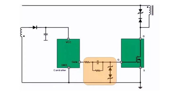
With unique device characteristics, GaN devices have been playing an increasingly heavy role in the fast charging field. However, the gate voltage of traditional GaN devices is very special, the threshold voltage of gate is extremely low, about 1v can partially conduct the gate voltage, and the gate withstand voltage is only about 6v.

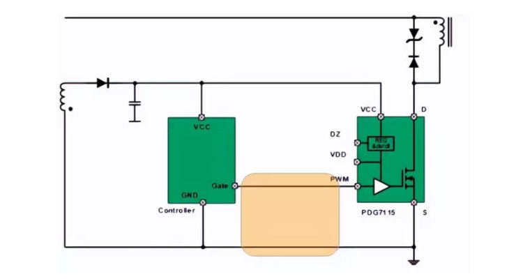
The diagram above shows the application circuit of traditional GaN devices. In order to match the traditional power controller, engineers need to configure complex level conversion circuit at the gate, which is very inconvenient to use.

Compared with traditional GaN devices, pgd7115 direct-drive gan power ICs do not need to configure complex level conversion circuits, so the peripheral circuits are more concise, which effectively reduces bom cost and accelerates the product time-to-market cycle.
With the advantages of fast switching speed, low resistance and low input and output charge, GaN is gradually replacing the traditional high voltage silicon mos tube in fast charging. The use of GaN instead of silicon mos tube not only reduces the switching loss, improves the conversion efficiency of the charger, eliminates the need to design a large heat sink, but also significantly increases the switching frequency of the power device, reduces the inductance of the transformer, reduces the size of the transformer, and thus reduces the size of the charger.

OEM GaN Charger Recommendation
The Advantage of ZONSAN's charger product:
1. overcurrent protection
2. input overvoltage protection
3. outut overvoltage protection
4. short circuit protection
5. overcharging protection
6. temperature protection
The Advantage of ZONSAN's charger product:
1. overcurrent protection
2. input overvoltage protection
3. outut overvoltage protection
4. short circuit protection
5. overcharging protection
6. temperature protection

Read More

Read More

Read More